When evaluating PCBA manufacturers, quality is generally an expectation, as it serves as your defense against field failures, warranty returns, and damage to your reputation. However, some manufacturers fall short. Siemens Manufacturing’s approach to inspection, testing, and engineering controls demonstrates what it takes to build quality into every assembly, rather than simply inspecting it at the end.
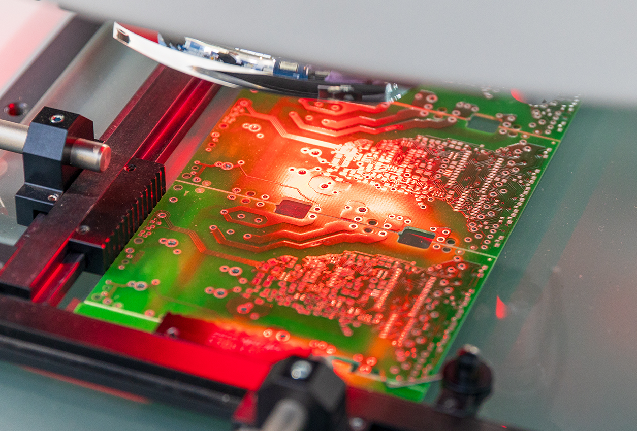
Automated Optical Inspection (AOI) Detects Problems Early For PCBA Manufacturers
In surface-mount technology, solder joints provide both electrical and mechanical connections between components and the PCBA. With the solder paste printing process, PCBA manufacturers deposit the solder paste (small particles of metal solder suspended in flux) on a printed circuit board (PCB) through a stencil, allowing for solder placement only where surface-mounted components will be located. Once the components are in place, the board is heated in a controlled manner, allowing the solder paste to melt and secure the components to the board. This is also referred to as reflow soldering. Issues with the solder joint can impact the functionality and reliability of the board. Automated Optical Inspection (AOI) is a tool used to prevent defects from progressing through the manufacturing process.
At Siemens Manufacturing, we integrate AOI at three distinct stages on each SMT line to catch defects as early as possible. It begins with solder paste inspection, which measures paste volume and area coverage to ensure each pad receives the correct amount of solder to form a solid joint. Insufficient paste can lead to weak joints, while excess paste risks bridging between components and causing short circuits. It has been determined that 52% to 71% of defects are attributed to the printing stage. By inspecting the paste immediately after stencil printing, Siemens prevents defects from moving downstream undetected.
The second AOI check comes after component placement and before reflow soldering. Here, AOI verifies every part is present, correctly oriented, and placed within tight positional tolerances. Components misaligned by even fractions of a millimeter can result in poor soldering or unreliable connections. This stage ensures that reflow only proceeds with properly prepared assemblies.
Finally, we use end-of-line 3D AOI after reflow to inspect solder joint formation, measuring height, volume, and fillet quality. These checks confirm that joints meet or exceed IPC standards for reliability and electrical performance. By having all three AOI types on every SMT line, Siemens creates a closed-loop inspection system, minimizing escapes and ensuring consistent assembly quality from the start of the line to final inspection.
X-Ray Analysis for Hidden Solder Joint Integrity
Not all solder joints are visible, especially with ball grid arrays (BGAs) and other bottom-terminated components common in today’s compact, high-density PCB designs. For these assemblies X-ray systems can validate production processes with non-destructive inspection of hidden joints. X-ray analysis reveals voids, insufficient solder, bridging, or misalignments beneath components that AOI cannot see.
This capability is critical for applications where failure isn’t an option, such as automotive control units, industrial safety systems, and medical electronics. Field failures from hidden solder joint defects can cost hundreds of times more to resolve than if detected during manufacturing. X-ray inspection ensures solder joints are structurally sound and meet IPC Class 2 or Class 3 standards as required, preventing latent defects from reaching your end users.
In-Circuit Testing: Detecting Electrical Faults at the Component Level
Functional tests confirm that a PCBA works as intended, but they don’t always pinpoint the root cause if a failure occurs. In-Circuit Testing (ICT) evaluates each component to ensure it is working. We use an Agilent 3070 In-Circuit Tester to perform parametric testing (component parameters, such as voltage, current, and resistance) of complex assemblies. ICT checks each resistor, capacitor, diode, integrated circuit (IC), and other components for value, orientation, and connectivity. And if it can’t reach a part physically, it uses JTAG testing to communicate directly to the chips through their own internal channels.
This testing approach isolates component-level faults quickly. For example, if a resistor is out of tolerance or an IC isn’t properly seated in its footprint, ICT identifies the exact failing node. Without it, diagnosing such issues during functional testing can be time-consuming and inefficient, resulting in delayed production and increased costs. In high-reliability sectors, these granular inspections give confidence that the PCB meets design specifications at every point, not just at the macro functional level.
PCBA Manufacturers Can Ensure Real-World Performance Through Testing
After AOI and ICT confirm visual and electrical integrity, we use functional testing to validate that assemblies operate under intended use conditions. Our engineering team designs custom test equipment to exercise specific circuit functions, including hipot (high-potential) tests for insulation resistance, RF test systems for communications modules, optoelectronic tests for sensor or display circuits, and analog and digital functional tests for general electronics.
We also perform Environmental Stress Screening (ESS). Our Thermotron environmental chamber subjects assemblies to controlled thermal cycling, revealing defects that only emerge under extreme temperature conditions. Likewise, electrodynamic vibratory testing simulates mechanical stress to expose solder fatigue, connector weaknesses, or other vibration-sensitive failures.
These ESS processes accelerate failure modes, acting as a time-compression tool to identify issues that might otherwise take months of real-world use to manifest. Identifying these problems in production rather than in the hands of customers reduces warranty claims and protects your brand reputation.
Engineering and Metrology: Controlling Quality at the Source
PCBA manufacturers understand that a good quality system not only prevents defects but also prevents them. This is why we integrate advanced metrology and engineering tools into our process to maintain dimensional and material accuracy.
Our OGP SmartScope CMM performs non-contact optical and tactile probe measurements to check PCB dimensions, mechanical parts, and prototype features against design tolerances. This is critical for boards that must fit precisely into housings, enclosures, or mating assemblies.
Incoming PCB lots are tested using a Phascope plating thickness measurement system to verify the copper and surface finish thickness across different date codes. Underspecified plating can lead to solderability issues, while excess thickness may affect fit and function. Verifying each lot ensures consistency and compliance before boards are ever entered into assembly.
Why Inspection and Testing Matter
These layered inspection and testing processes directly affect the total cost of ownership. Poor quality assemblies from other PCBA manufacturers result in assembly line stoppages, field returns, customer dissatisfaction, and lost contracts. Our inspection and testing provide confidence in the design’s real-world performance, especially in harsh or safety-critical environments.
Our integrated AOI, X-ray, ICT, functional testing, and ESS demonstrate a proactive approach to quality. It’s not just about passing IPC standards. It’s about ensuring the board you spec today performs to your expectations tomorrow.
If you’re evaluating PCBA manufacturers, consider their inspection and testing infrastructure as seriously as their quoting speed or unit cost. Our layered quality approach reduces risk, protects uptime, and ensures your products meet the standards your customers demand.