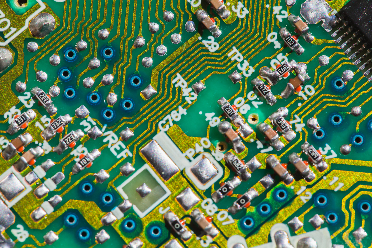
For applications requiring reliable circuit boards, through hole PCB assembly is an ideal manufacturing solution. This process plays a vital role in modern electronics and can improve the durability and strength of these products, which is crucial in high-stress applications. This method involves mounting leaded electronic components onto a circuit board, which includes drilling holes and soldering.
If you’ve ever wondered how to maintain the quality of electronic products over an extended period of time, through hole assembly is a top-tier choice. Let’s explore the process of through hole PCB assembly and how Siemens Manufacturing supports clients with our high-quality services.
A Closer Look at Through Hole PCB Assembly
The process starts with bare PCBs including holes that are plated and connected to board traces. Components are then inserted into those holes and soldered to the pads on the bottom side of the printed circuit board. Through hole assembly offers several key benefits, including:
Enhanced Mechanical Strength and Durability
This process provides a stronger mechanical bond compared to surface-mount components, making it ideal for applications that are subjected to mechanical stress or vibration. Some examples here include inductors, large capacitors, and more.
More Reliability, Especially in High-Stress Applications
Through hole assembly ensures more reliability, especially in demanding environments, and also reduces the risk of joint failure under stress. As a result, this process is commonly used in industrial equipment, automotive electronics, and aerospace products.
Easier Prototyping
Component placement is easier in the through hole process, making prototyping simpler. Because of the larger size of through hole components, rework is also easier.
Compatibility with Larger Components
Some electronic components demand through hole packages because of their size and weight. This includes large capacitors and transformers, and through hole assembly allows the durable mechanical support that is needed to securely mount these heavier components onto the circuit board.
Cost-effectiveness
Through hole assembly is ideal for lower volume production or for larger components, which may have higher placement costs associated with automated surface mount assembly equipment.
This process first starts with a Design for Manufacturability (DFM) and Bill of Materials (BOM) review, which allows experts to evaluate each aspect of design, including materials, before continuing. Components are then procured and inventory management begins, reducing waste and improving costs.
Using both manual and automated processes, components are placed and the soldering process begins. Several soldering processes are available based on the board layout and production volume, such as:
- Wave Soldering: This is the most common method for high-volume through hole assembly. The PCB, with components inserted and secured, is passed over a wave of molten solder. The solder wave contacts the underside of the board, wetting the component leads and the corresponding pads, creating a strong solder joint. Flux is applied to the board before it enters the solder wave to clean the surfaces and promote proper wetting.
- Selective Soldering: This method is used for PCBs with a mix of through hole and surface mount components, or for specific areas where wave soldering is not suitable. Automated soldering heads selectively apply solder to individual through hole joints.
- Manual Soldering: For prototyping, low-volume production, or rework, manual soldering using a soldering iron is often employed. A skilled technician applies heat to the joint and then introduces solder wire, allowing it to flow and create a reliable connection.
Finally, inspection and quality control procedures begin to ensure the product will perform as required. Your product might also need cleaning and finishing processes, including conformal coating, before packaging and delivery.
The through hole PCB assembly process creates reliable, durable assemblies that can withstand harsh environments, making this method well-suited for industrial applications. This process requires an expert manufacturing partner. That’s where Siemens comes in.
How Siemens Manufacturing Can Enhance the Through Hole PCB Assembly Process
For over 60 years, Siemens Manufacturing has been on the forefront of custom electronics manufacturing. We provide solutions that meet our customers’ toughest challenges, and our through hole PCB assembly services are comprehensive and robust. Our capabilities include eight wave solder lines between all of our facilities, four selective solder lines, robotic soldering, two axial insertion machines, and two DIP insertion machines. All of this enables us to provide efficient and high-quality services, and we are able to work with tens of thousands of boards per day.
In addition to our through hole assembly services, we also offer surface mount assembly, BGA assembly, box build assembly, and more. We ensure your product is finished to your exact specifications with our conformal coating and product testing services. In all that we do, we seek to ensure your precise vision is brought to life because we understand how important it is that your product performs as expected.
No matter the application, we can tackle your most difficult EMS problems. With our experience with various markets, such as automotive, industrial, construction, military, and more, we are the ideal partner for your next project. We offer flexible support, and low- to high-volume options, and with our design support and dedication to customer support, you never have to worry about your project’s success.
Are you ready to elevate the standard of your electronics manufacturing? Connect with Siemens today for a quote.
