
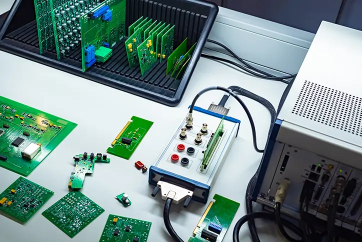
Testing is one of the last opportunities to catch defects before a PCBA leaves the production floor. The right test strategy reduces field failures, shortens troubleshooting times, and gives manufacturers confidence that every assembly performs as intended. Functional testing services and in-circuit testing (ICT) are two common test methods.
Although they are often mentioned together, they serve different functions. Understanding the difference helps OEMs determine which approach fits their product, production volume, and quality requirements.
What Is In-Circuit Testing?
In-circuit testing verifies the electrical integrity of an assembled PCB by testing individual components and connections. Using a bed-of-nails fixture or flying probe system, the tester accesses specific test points on the board to measure electrical characteristics. ICT can detect problems such as:
- Open circuits
- Short circuits
- Missing components
- Incorrect component values
- Reversed polarity
- Soldering defects
- Some programming and digital logic issues
Because ICT isolates individual components, it is excellent at identifying the exact location of a manufacturing defect. Instead of knowing that a board failed, production personnel know which resistor, capacitor, integrated circuit, or solder joint caused the failure.
What are Functional Testing Services?
While in-circuit testing evaluates individual components, functional testing services help answer the question, “Does the assembled product actually work?” Functional testing validates the completed assembly and ensures it performs as designed. Test equipment may simulate sensors, communications, user inputs, or operating conditions while measuring outputs and system behavior.
Functional testing services may verify:
- Power-up sequences
- Analog and digital outputs
- Communications ports
- Firmware operation
- Sensor inputs
- Display operation
- Motor or actuator control
- RF performance
- Overall system functionality
Unlike ICT, functional testing evaluates the board as a complete system instead of examining individual electrical connections.
In-Circuit Testing vs. Functional Testing Services
The easiest way to understand the difference is by considering what each method is designed to detect.
| Feature | In-Circuit Testing | Functional Testing |
|---|---|---|
| Primary Purpose | Verify assembly quality | Verify product operation |
| Tests Individual Components | Yes | No |
| Tests Finished System Behavior | No | Yes |
| Finds Exact Manufacturing Defects | Excellent | Limited |
| Requires Custom Fixtures | Often | Often |
| Requires Product Firmware | Usually No | Usually Yes |
| Best For | High-Volume PCB Production | Final Product Validation |
The two methods complement one another rather than compete.
When In-Circuit Testing Makes Sense
ICT works especially well when manufacturers produce moderate to high volumes of the same PCB. Although fixture development requires an upfront investment, the actual test cycle is fast, often taking only seconds per board.
Manufacturers frequently choose ICT when:
- Production volumes justify fixture costs.
- Fast fault isolation is important.
- Boards contain many discrete components.
- High yields are required.
- Manufacturing defects must be identified quickly.
For products built in large quantities, rapid diagnosis can significantly reduce repair time and production costs.
When Functional Testing Services Is the Better Choice
Functional testing services becomes more valuable when real-world performance matters more than locating a specific assembly defect. It is often the preferred choice for products that include:
- Embedded software
- Microcontrollers
- User interfaces
- Communications protocols
- Complex power management
- RF circuitry
- Custom operating sequences
Many defects cannot be detected solely by checking component values. A board may pass every electrical test yet still fail due to firmware issues, timing problems, or incorrect system interactions. Functional testing verifies that the customer receives a product that behaves as expected under operating conditions.
Why Many Electronics Manufacturers Use Both
The highest level of quality often comes from combining multiple inspection and test methods throughout production. A typical workflow may include:
- Automated Optical Inspection (AOI) after SMT assembly to detect placement and solder defects.
- In-circuit testing to verify component installation and electrical integrity.
- Functional testing to confirm the completed assembly performs correctly.
- Burn-in, environmental stress screening (ESS), thermal, or RF testing when required by the application.
Each stage catches different types of defects before products move to the next manufacturing step.
Factors That Influence Test Strategy
No single testing method fits every product. Several considerations influence the best approach.
- Production volume— High-volume products often justify ICT fixtures because the tooling cost is spread across many assemblies. Lower-volume builds may rely more heavily on functional testing or flying probe inspection.
- Board complexity—Dense, highly integrated boards may require a combination of electrical, optical, and functional verification.
- Regulatory requirements— Medical, industrial, aerospace, and automotive electronics frequently require multiple validation methods to meet customer or industry standards.
- Product maturity— Early prototypes may rely primarily on functional testing, while mature production programs often add ICT as volumes increase.
Choosing the Right Testing Partner
Effective testing starts long before production begins. An experienced electronics manufacturing services (EMS) provider can recommend a test strategy based on the product’s design, production volume, reliability requirements, and expected lifecycle.
At Siemens Manufacturing, quality verification includes comprehensive product testing supported by component-level lot traceability, automated optical inspection, Agilent in-circuit testing, functional testing, and additional capabilities such as burn-in, RF, environmental stress screening (ESS), and thermal testing when required. This layered approach helps identify manufacturing defects early while confirming that finished assemblies perform as intended.
Contact us to talk about your next PCBA project.
Frequently Asked Questions
Is in-circuit testing better than functional testing?
Neither is inherently better. ICT verifies that the PCB has been assembled correctly, while functional testing verifies that the finished product operates correctly. Many manufacturers use both.
Can a board pass ICT and still fail functional testing?
Yes. ICT may confirm that components are installed correctly, but it cannot detect every firmware issue, software defect, timing problem, or system-level interaction.
Does every PCB require in-circuit testing?
No. Low-volume products, prototypes, or assemblies without sufficient test access may use flying probe inspection, functional testing, or other verification methods instead.
Why do some manufacturers perform multiple tests?
Each testing method identifies different failure modes. Combining AOI, ICT, and functional testing provides broader defect coverage and reduces the likelihood that faulty products reach customers.