Custom electronics manufacturing services play a crucial role in delivering reliable and high-quality electronic products across a wide range of industries. By focusing on rigorous testing and quality assurance processes, these services ensure that every component and assembly meets exacting performance standards. In this article, we’ll explore how advanced inspection and testing techniques contribute to superior outcomes in custom electronics manufacturing.
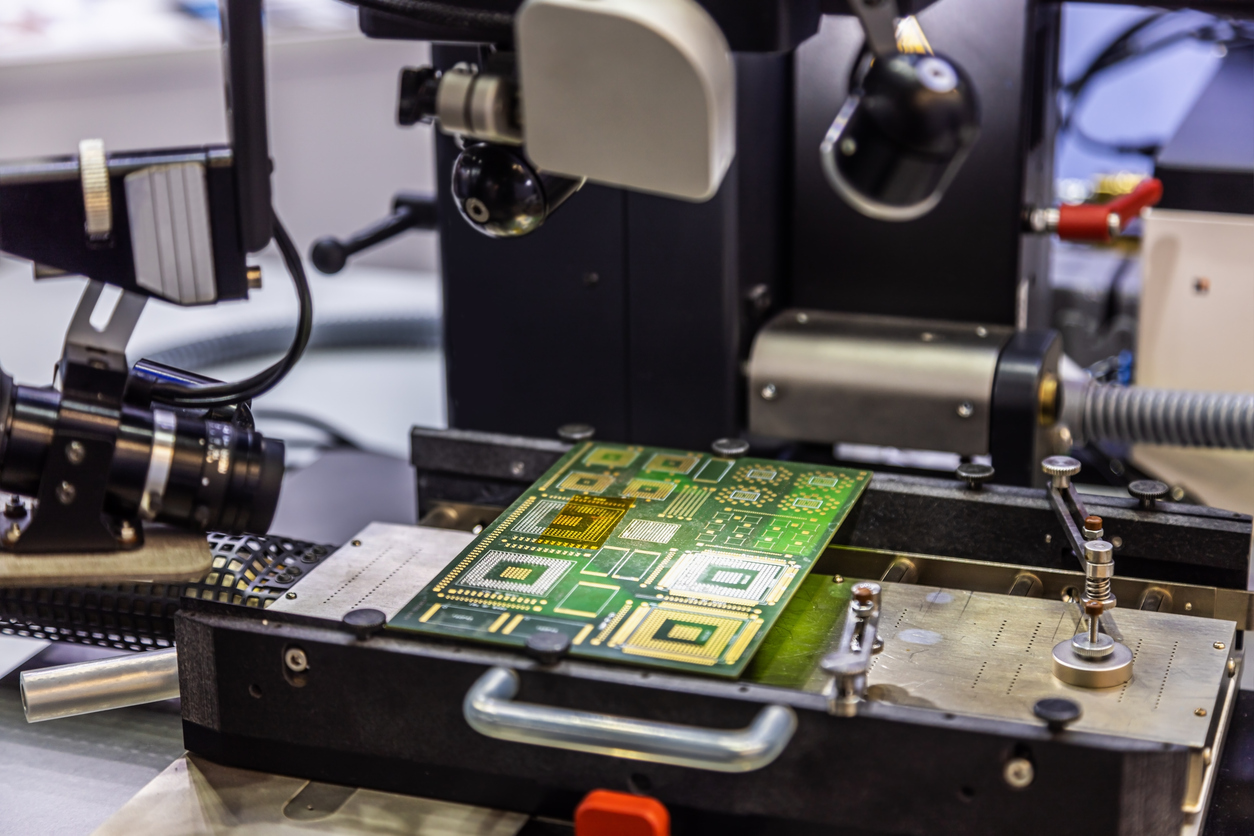
Automated Optical Inspection (AOI)
Automated optical inspection (AOI) improves electronics manufacturing by automating defect detection and supporting consistent, repeatable inspection results. In a typical SMT process, AOI can be used at multiple points: solder paste inspection after paste print, pre-reflow inspection after component placement, and end-of-line 3D AOI after reflow. These inspections help identify issues early and confirm solder joint quality so assemblies meet or exceed IPC workmanship standards.
AOI programs verify that components are present, placed accurately, and oriented correctly (including polarity where applicable). When parts include readable markings, AOI can also help confirm correct part identification or marking orientation. This is especially useful for builds that share a common bare PCB but have different component populations, because AOI can confirm the correct variant is assembled.
The AOI is equipped with side-view cameras, which allow for a greater inspection profile, providing several advantages:
- RF shield frame inspection: Side-view optics help inspect solder fillets and component terminations near shield frames and other overhangs where a purely top-down view can be limited.
- PLCC & J-lead inspection: Angled cameras improve visibility of fillets and lead conditions on packages where solder connections are partially hidden from a straight top-down view.
- Tall component shadowing: Side views reduce inspection blind spots caused by tall parts (for example, large capacitors or connectors) that can shadow nearby components.
- Lifted lead detection: Angled views can help identify lifted leads on gull-wing and J-lead devices that may be difficult to confirm with a direct overhead image.
Electrical Testing & Test Engineering
Beyond visual inspection, electrical testing confirms that the assembly performs as intended and helps detect defects that may not be visible (e.g., opens, shorts, incorrect values, or intermittent errors). Manufacturers often develop and maintain custom production test fixtures and automated test stations to run tests quickly and consistently at the right point in the process (during board build, at end-of-line, or after final assembly). Depending on the product, this can include safety testing (such as hipot), RF verification, optoelectronic checks, and analog/digital functional testing, each chosen to reduce defects that reach the customer and improve first-pass yield.
In-circuit testing (ICT) is commonly used on complex assemblies to perform fast, repeatable parametric measurements at the component and electrical-connection levels (i.e., a net on the PCB). This helps detect and isolate issues early, such as shorts between nets, opens on a net, wrong values, missing parts, and some solder-related defects, so troubleshooting is faster and downstream functional test time is reduced.
Quality & Reliability Screening
In custom electronics manufacturing services, quality is typically built through layered controls that progress from verifying inputs to validating outputs. EMS providers will typically address it by (1) confirming incoming materials and PCBs meet spec, (2) using targeted inspection methods to verify workmanship where defects can be hidden, and (3) applying screening when needed to increase confidence in reliability for demanding environments. The methods below are commonly used together because each addresses a different risk.
As an example of targeted, non-destructive verification, X-ray inspection can be used to detect hidden or hard-to-see solder joints (e.g., BGAs and other area-array packages). It helps confirm solder joint integrity, investigate suspected defects, and expedite root-cause analysis when optical inspection can’t fully see the connection.
Upstream of assembly, dimensional verification and incoming quality checks help ensure parts meet requirements before they enter production. Optical/probe measurement systems (often used like a CMM) can verify PCB dimensions and mechanical parts, supporting both engineering development and ongoing process control. Plating thickness measurement is another common incoming check for PCB lots, helping confirm that critical finishes meet specification and supporting long-term reliability.
After boards pass inspection and electrical test, some programs add an additional layer: environmental stress screening (ESS). When required, ESS helps reduce the likelihood of early-life field failures by revealing weaknesses at production. Thermal screening uses controlled temperature cycling and soaking to expose issues such as marginal solder joints or temperature-sensitive components, while vibratory screening applies controlled vibration to uncover mechanical or intermittent defects. ESS is most effective when it’s tied to clear acceptance criteria and paired with appropriate electrical tests before and after the stress.
Ready to Improve Quality Outcomes? Custom Electronics Manufacturing Services with Siemens
Quality should reduce risk throughout the build by catching defects as early as possible (not just at the end), using the right method for the right failure mode, and feeding results back into process improvements. Siemens Manufacturing applies this layered approach within its custom electronics manufacturing services, supporting customers from early builds through sustained production with documented inspection plans, production-ready test fixtures, and quality controls aligned to product requirements. Whether your priority is higher first-pass yield, fewer customer returns, or additional screening for harsh environments, the right combination of inspection and test can be tailored to match your risk profile and compliance needs.
Want to review your current test and inspection strategy? Contact Siemens Manufacturing to discuss your product, quality goals, and production volumes. We’ll help you define the right mix of AOI, electrical test, and screening to reduce risk and improve outcomes.