
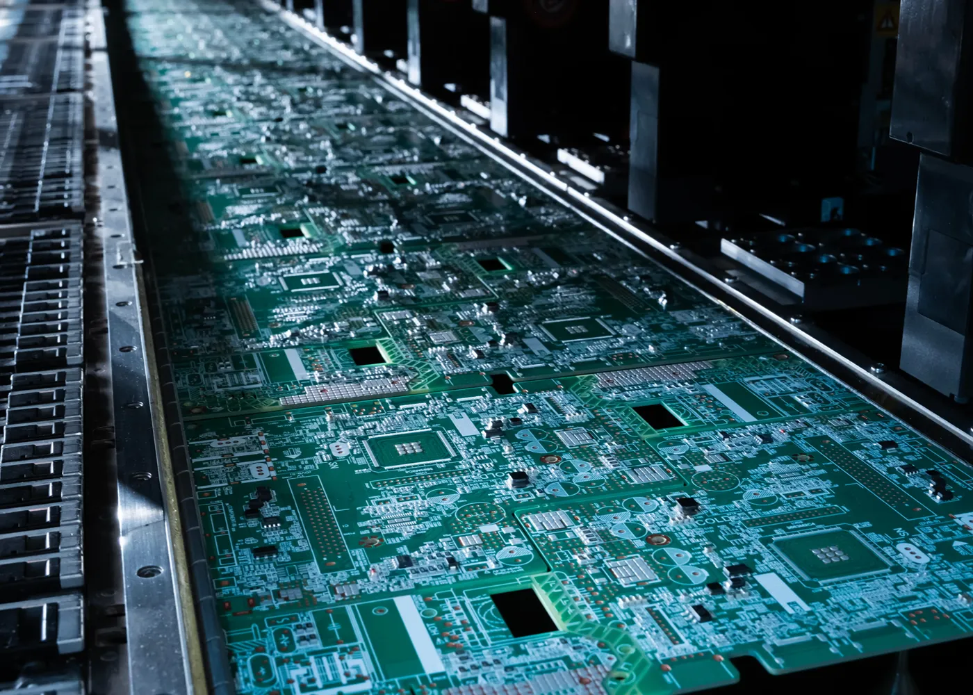
Every reliable circuit board starts with its construction. For manufacturers producing electronics at scale, the assembly stage determines whether design intent holds up under real-world conditions or leads to complete or intermittent failure. That’s why surface mount technology assembly has become the standard approach for producing PCBs that perform consistently, from prototype runs to high-volume production.
What Is Surface Mount Technology Assembly?
Surface mount technology assembly is the process of mounting electronic components directly onto the surface of a printed circuit board, rather than inserting component leads through drilled holes, as in through-hole technology. Solder paste is printed onto designated pads, components are placed using automated equipment, and the board then passes through a reflow oven, where controlled heating melts the paste to form permanent electrical and mechanical connections.
SMT has become the dominant method in PCB assembly because it supports smaller components, tighter spacing, and faster production without sacrificing the durability electronics need in the field. But its advantages go beyond speed and size. Done correctly, SMT assembly is one of the biggest drivers of a finished board’s long-term reliability.
Precision Placement Reduces Defects at the Source
Manual component placement introduces variability, such as small misalignments or inconsistent pressure. Automated pick-and-place equipment removes most of that variability, positioning components with a level of accuracy and repeatability manual assembly can’t match. This consistency is critical in designs with fine-pitch components, where even a slight misalignment can turn into a bridged or open connection later on.
Placement accuracy also affects orientation, spacing, and contact with the solder paste. Those details determine whether a component sits flat, forms a clean solder joint, and remains stable as the board moves into reflow. On dense PCB layouts, that control becomes more important because small passive components and fine-pitch integrated circuits leave little room for placement error.
Controlled Reflow Improves Solder Joint Consistency
Solder joint quality depends heavily on how a board moves through reflow. Temperature ramp rates, soak times, peak temperature, and cooling rates must match the specific components, board design, solder paste, and materials being used. During reflow, the solder paste must heat evenly, activate the flux, remove surface oxides, and allow the molten solder to properly wet component leads and PCB pads. If the thermal profile is too aggressive or insufficient, solder may not flow as intended, resulting in weak or inconsistent intermetallic bonds.
A properly controlled reflow profile promotes consistent wetting, solder spread, and joint formation across the entire assembly. It also accounts for variations in component mass and board density, ensuring that large and small components reach the required temperatures at the appropriate time. When thermal conditions are controlled and repeatable, manufacturers can reduce defects such as cold joints, tombstoning, solder bridging, head-in-pillow defects, and excessive voiding. The result is stronger, more reliable solder connections that better withstand thermal cycling, vibration, and long-term field use.
Inspection and Testing Confirm the Build Before Shipment
Reliable SMT assembly does not end when components are placed and soldered. Inspection and testing confirm the assembly meets build requirements before it leaves production. Automated optical inspection can be used at multiple stages, including after solder paste printing, after component placement, and after reflow. These checks help identify missing parts, shifted components, polarity issues, solder defects, and other workmanship problems while the board is still in production.
For components or solder joints that cannot be fully verified from above, additional inspection methods may be needed. Side-view optics can improve visibility around shield frames, J-leads, tall components, and lifted leads. X-ray inspection is used when solder joints are hidden underneath packages such as BGAs. Electrical testing then confirms whether the finished assembly performs as intended, helping catch opens, shorts, incorrect values, or intermittent faults that may not be visible during optical inspection.
Want a deeper look at electronics testing and quality assurance? Read Testing and Quality Assurance in Custom Electronics
High-Density PCB Layouts Depend on Process Control
Surface mount technology assembly makes compact PCB layouts possible by allowing smaller components, tighter spacing, and placement on both sides of the board. That density increases the need for controlled paste printing, accurate placement, stable reflow, and layered inspection. As board space gets tighter, small assembly variations have less room to hide and can create defects that affect reliability later.
Built for Reliability, From First Placement to Final Inspection
A board that passes inspection still must perform under vibration, temperature changes, humidity, and over its long service life. Controlled placement, reflow, and inspection reduce the chance that small assembly defects become intermittent field failures. For products where electronics failure can cause downtime, service issues, or recalls, assembly discipline is part of the reliability case.
At Siemens MFG, we build reliability into the surface mount technology assembly process, so customers can feel confident in their board’s performance. If you’re evaluating a partner for your next PCB assembly run, we’re happy to review your specifications and show how our process supports the reliability your product needs.